
Applications
- Cristallinity of Polysilicon
-
Background
a-Si has opened up a new application field such as solar cell and liquid crystal devices. Trasisters can be made relatively easily by using the amorphous silicon (a-Si).
Although a-Si is easy to process, it has low electron mobility, so its performance as a transistor is insufficient. Therefore, replacement of a-Si to polysilicon (p - Si) is proceeding.
p-Si is equivalent to intermediate between a-Si and c-Si and consists of grains of single crystal having different orientations. In the case of p - Si, electrons are scattered at grain boundaries, so that electron mobility is lower than c - Si but electron mobility is much larger than a - Si.In order to improve this electron mobility, it is necessary to improve the crystallinity of p - Si (that is, to enlarge the grain size of the single crystal). Annealing is used for improving the crystallinity of p - Si, especially laser annealing which can perform spot processing in a short time and has little influence on other parts is often used.
Meanwhile, as well as improving crystallinity, it is also necessary to manage the variation, and it is required to be able to feedback on the spot on the occasion of management of individual crystallinity and annealing.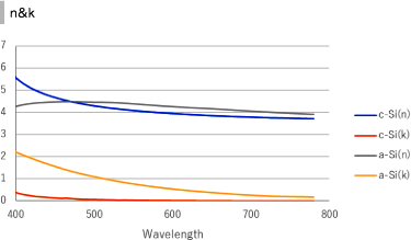
Crystallinity and refractive index
Since c-Si and a-Si have completely different crystallinity, their electrical and optical properties also differ.
The graph on the right shows the refractive indices of c-Si and a-Si.p-Si takes intermediate between c-Si and a-Si depending on its crystallinity.
If the crystallinity is 0%, it becomes a-Si, and if the crystallinity is 100% it becomes c-Si.
This means that p-Si can be approximated as a composite of c-Si and a-Si. As such a theoretical model, effective medium approximation (EMA) is often used.Result
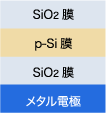
Evaluate the crystallinity of the p-Si film with the structure as shown on the right.
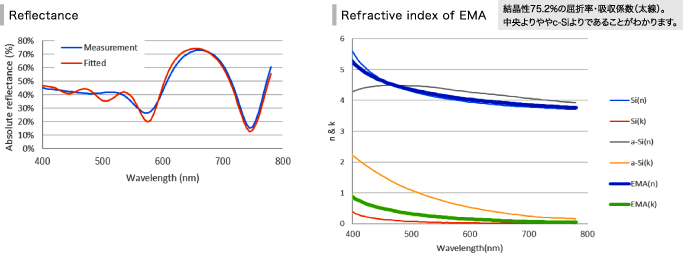
The unknown parameters are the crystallinity of the p-Si film, the film thickness of p-Si, and the film thickness of SiO2 above and below p-Si.The lower left blue line is the measured reflectance and the red line is the calculated waveform when fitting unknown parameters. Finally, the following values were obtained for each parameter.
- Crystallinity: 75.2%
- Thickness of p-Si: 188.4nm
- Thickness of lower SiO2: 148.6nm
- Thickness of upper SiO2: 2.5nm
- Density evaluation of porous film
-
Background
Low-k is a meterial with a small dielectric constant relative to silicon dioxide. It is used as an interlayer insulating material of LSI wiring layer.
By using Low-k material, capacitance between interconnects can be lowered, and LSI with high speed and low power consumption can be realized.
Conventionally, SiO 2 was used as an interlayer insulating material, and its relative dielectric constant is about 4.2 to 4.0.
To reduce the relative dielectric constant, we use the porous material containing air.
Meanwhile, with the nanoporous structure, there is a problem of deterioration of mechanical strength and reliability, and management in the production process is required.Modeling and anaalysis of Low-k film

The low-k film can be regarded as a mixed material of SIO 2 film and air. It is possible to estimate density and refractive index from the mixing ratio.
The film thickness monitor can measure the mixture ratio (density) and film thickness separately if the target layer has sufficient film thickness.The lower left graph shows the spectral reflectance when the film thickness is changed for a Low-k film with a film thickness of 100 nm and a density of 50%.
Also, the lower right graph shows the density of the low-k film with film thickness of 100 nm and density of 50%.
From the each signal difference, it can be seen that separation measurement of film thickness and density is possible.
Also, film thickness resolution is under 1 nm and the density resolution is under 1% .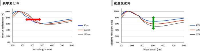
- Nano line width measurement
-
Background
In the recent lithography process in semiconductor manufacturing, it is essential to measure the critical dimension (CD) of a nanoscale circuit pattern, and CD-SEM and AFM have been used. In recent years, OCD (Optical Critical Dimension) that measures CD by using light scattering is emerging, especially at the production site. This is also called scatterometry.
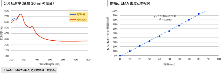
This OCD system consists of a spectroscopic ellipsometer with a high throughput and a small spot and an computing unit that performs parameter fitting at high speed using RCWA (rigorously coupled wave theory), and it is highly specialized.
Here, we will explain a method of measuring line width easily using EMA.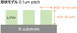
Modeling and Correlation between EMA and RCWA
We approximate the nano line width as shown on the left figure using EMA. The resist layer can be approximated as a mixture of resist and air, and its density is proportional to line width.
The following graph plots the mixing ratio obtained by EMA against the actual line width, which shows that it is in a linear relationship. Also in this case, We can see that line-width (i.e. density ) and film thickness can be measured at the same time.
- Complex film structure
-
In the case of the following complex pattern, the film thickness of each layer and the etching depth can be obtained simultaneously from the reflection spectrum. This is also applicable to MEMS and trench structure.
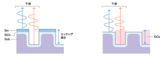
The physical model to be applied varies depending on the size and shape as follows.
① Effective medium (EMA) theory
② Mutual interference theory of Fresnel multilayers
③ Rigorous coupled wave (RCWA or FMM) theory
(solves the Maxwell equation correctly using fourier approximation. Periodic pattern is necessary.)Our film thicknesss monitor can create the recipe beased on ① and ②.
Recipe ③ is provided as pre-calculated data for each measurement target. Just inquire about actual applicability.
- Battery electrode
