


PRODUCT INFORMATION
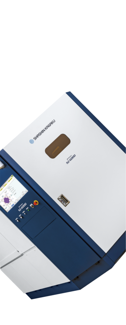
 Planetary
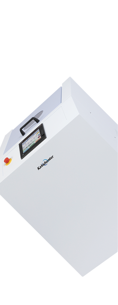
Centrifugal Mixer
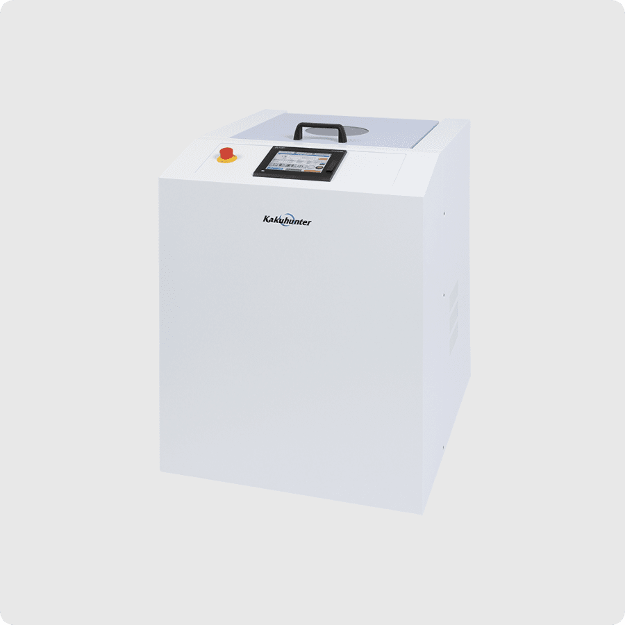
Kakunter is a mixer that simultaneously mixes and defoams materials.With the bubble breaking effect by the shearing force and material film forming action created by the combination of revolution and rotation, simultaneous processing of precise mixing and defoaming can be performed in a short time.
Stereolithography 3D Printer
for Ceramics
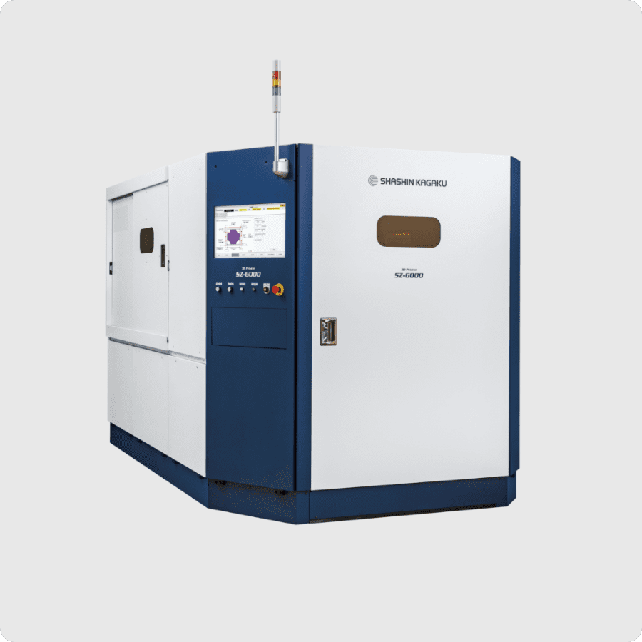
Our stereolithography 3D printer for ceramics suits from R&D through mass production in various industries. It realizes high-definition and high-precision modeling designs of complex structures which cannot be realized with conventional modeling method.
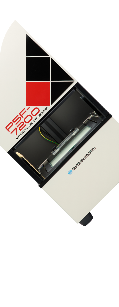
Automated Colony Counter
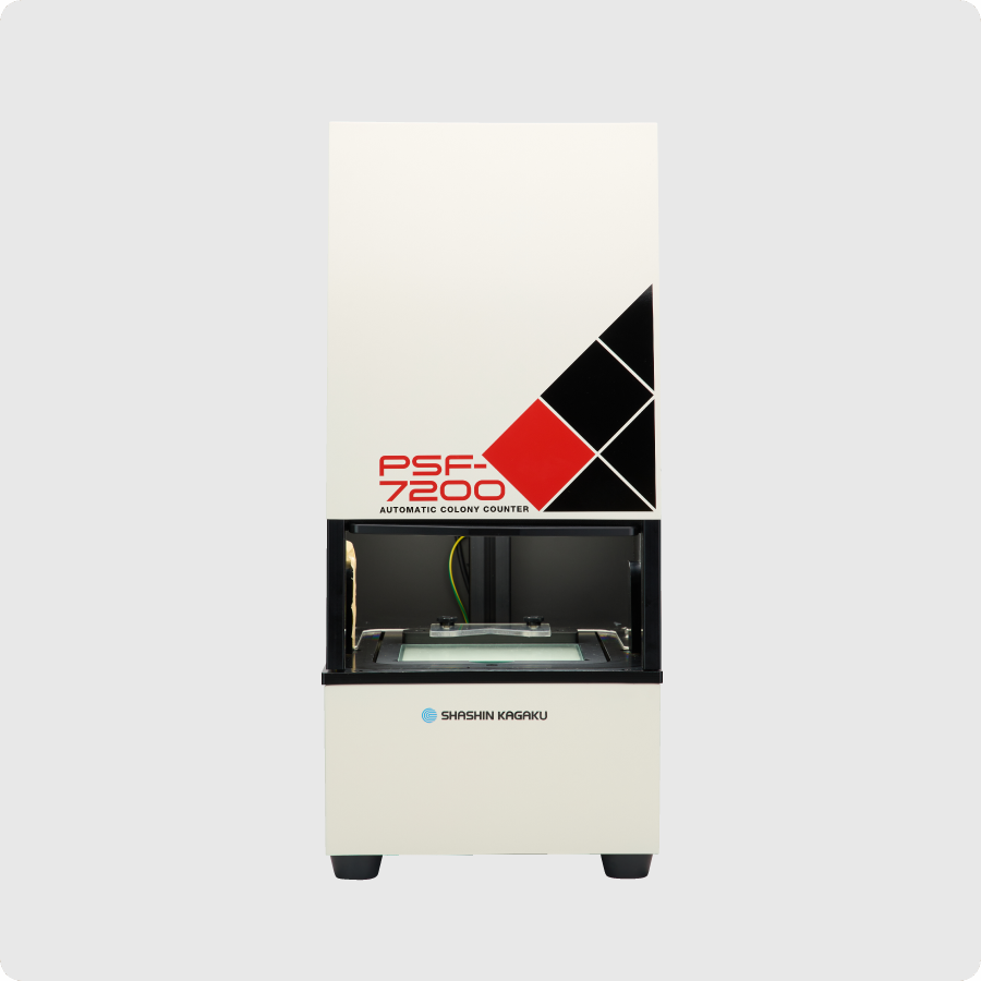
Automated colony counters are used for microorganism testing. Accurately measure colony counts in seconds and automatically generate reports.The counting time can be greatly reduced.
Precision Automatic Measuring
Machine
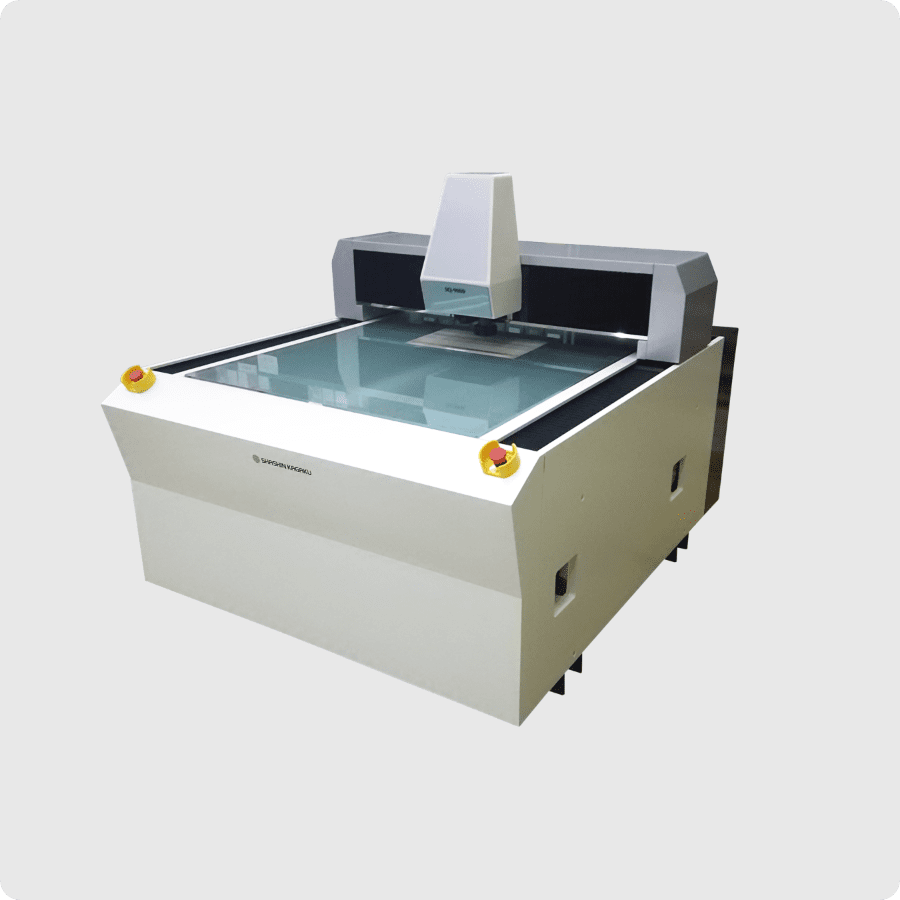
A non-contact measuring device for dimensions of substrates, films, stainless steel / nylon mesh, screen masks, etc.Image analysis software makes it possible to confirm the shape and surface of objects and to perform 3D measurements using the “focusing method.”
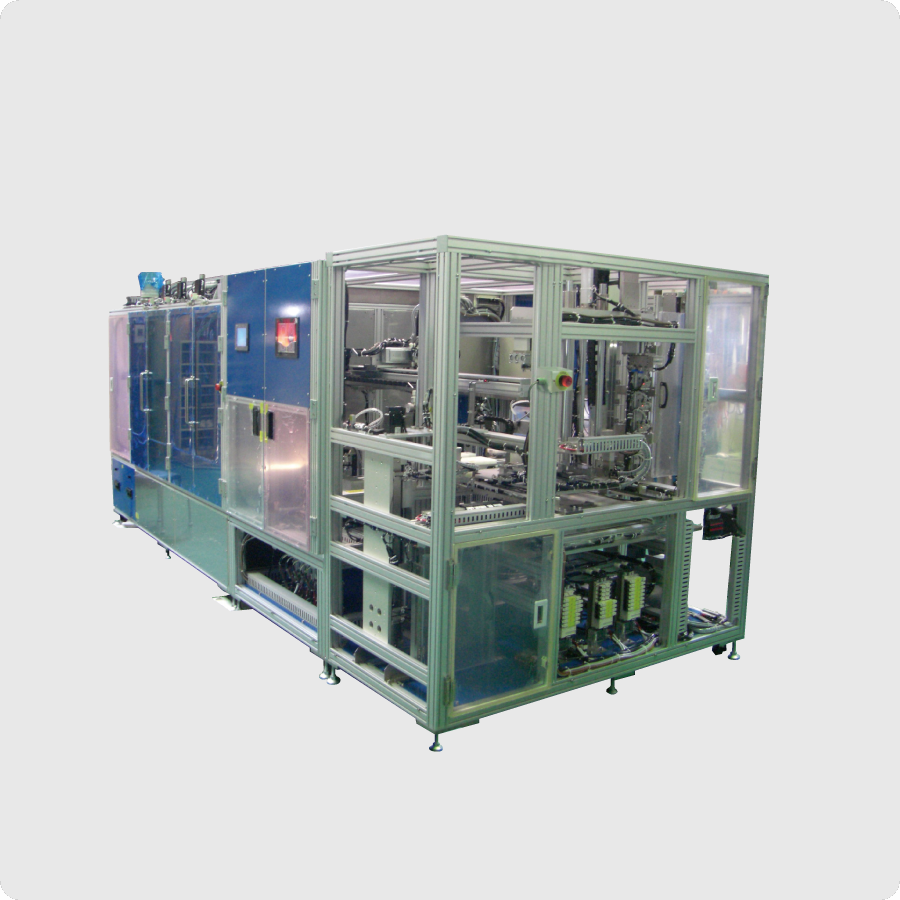
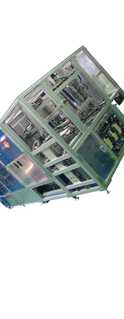
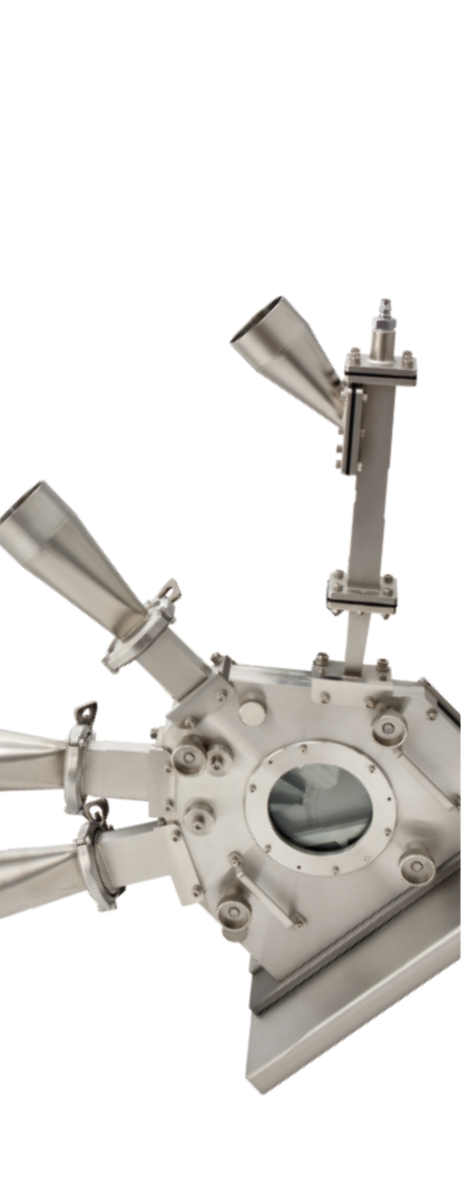
Factory Automation
We will meet our customers’ requests, “in the most optimal way,” for lithium ion secondary battery manufacturing line, material handling equipment, welding equipment, vacuum equipment, and so on.We offer a wide range of services, including periodic support, remodeling, and extension after delivery.
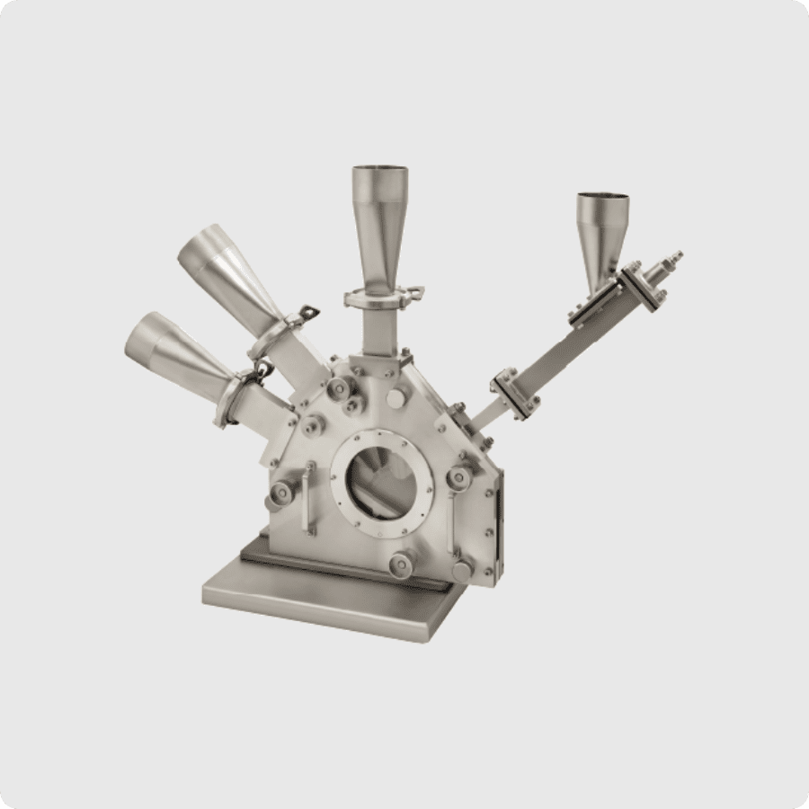
High Precision Coanda Classifier
High Precision Coanda Classifier “HIPREC” is an air current classifier which effectively obtains three products: fine, medium and coarse powder at one time, by applying the characteristic of powder flowing along the wall surface.High dispersion nozzle of the material supplying part makes highly efficient classification performance possible.
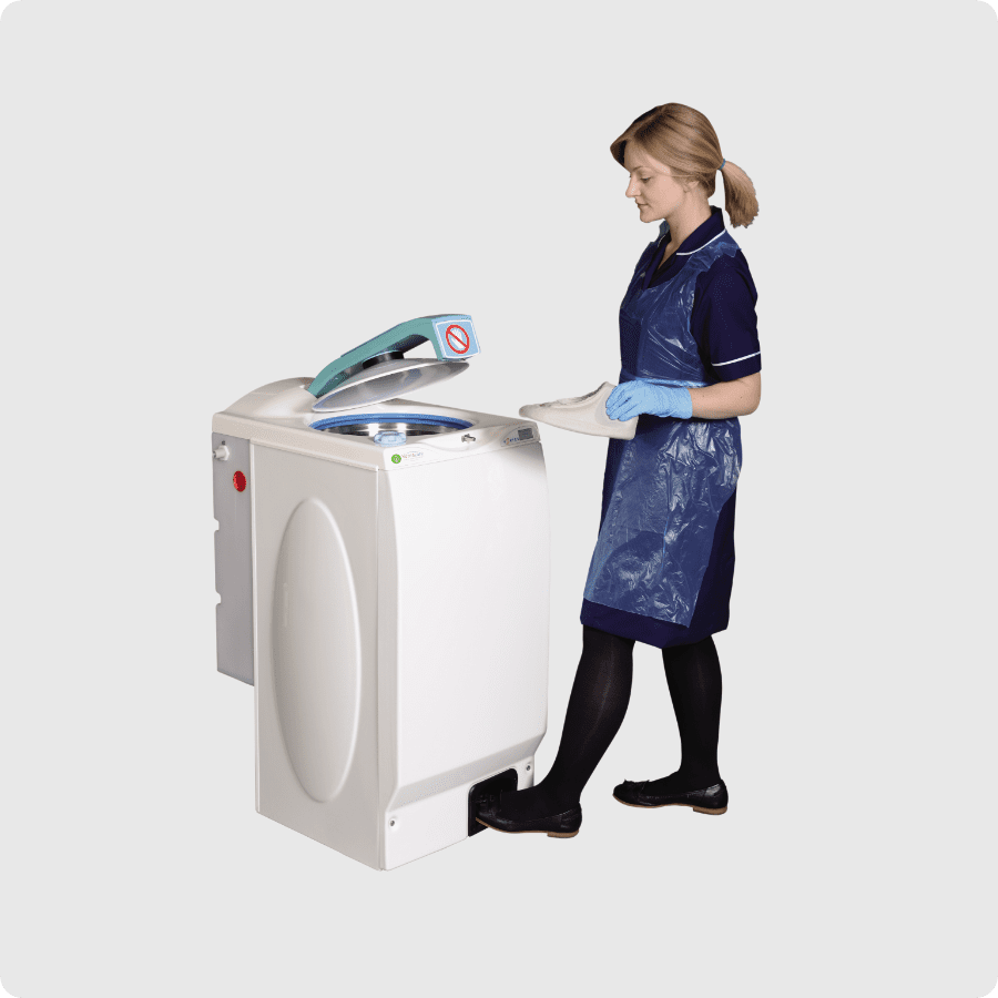
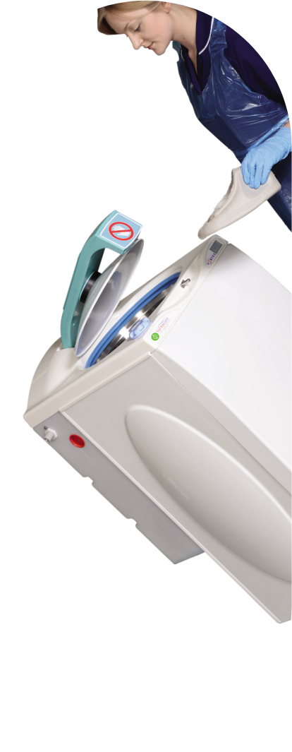
Health Care
We are developing businesses based on the keywords of “work reduction,” “infection control,” and “improvement in the working environment” for people working in medical and nursing care facilities.We offer products that increase the amount of time with patients and are appreciated by both patients and caregivers.


NEWS
Forum Labo 2020, France (2020, March 26-28th, Lyon) was cancelled for COVID-19.
Euro Lab 2020, Poland (2020, March 17-19th, Warsaw) was cancelled for COVID-19.
We have newly obtained CE Certification for SK-2000T, planetary Mixer.
We have newly obtained CE Certification for SK-1100T, planetary Mixer.
We exhibit at Manufacturing 2018, Thailand (2018, June 20-23rd, Bangkok). We are welcomed to visit at our booth.
We exhibit at Achema 2018, Germany (2018, June 11-15th, Frankfurt). We are welcomed to visit at our booth.
We exhibit at ICMAT 2018, Singapore (2018, June 17-22nd, Singapore). We are welcomed to visit at our booth.
We exhibit at Coating & Corrosion Show Malaysia 2018, Malaysia (2018, May 17-19th, Kuala Lumpur). We are welcomed to visit at our booth.
We exhibit at Cosmo Beauty 2018, Korea (2018, May 9-11th, Seoul). We are welcomed to visit at our booth.
We exhibit at Nano Tech Malaysia 2018, Malaysia (2018, May 7-9th, Kuala Lumpur). We are welcomed to visit at our booth.
We exhibit at IndustriTech 2018, Thailand (2018, April 27-29th, Khonkaen). We are welcomed to visit at our booth.
We exhibit at India Lab Expo 2018, India (2018, April 25-26th, Mumbai). We are welcomed to visit at our booth.
We exhibit at Korea Lab 2018, Korea (2018, April 18-20th, Seoul). We are welcomed to visit at our booth.
We exhibit at Medtec 2018, Germany (2018, April 17-19th, Stuttgart). We are welcomed to visit at our booth.
We exhibit at Fine Chemicals Japan 2018, Tokyo (2018, April 18-20th, Tokyo Big site #East 1Hall FA-01). We are welcomed to visit at our booth.
We exhibit at Automach 2018 (2018, March 28-30th, Chonburi). We appreciate to visit us there.
We exhibit at Coating Korea, 2018 (2018, March 28-30th, Seoul). We appreciate to visit us there.
We exhibit at Forum Lab, 2018 (2018, March 28-30th, Lyon). We appreciate to visit us there.
We exhibit at SEMICON China, 2018 (2018, March 14-16th, Shanghai). We appreciate to visit us there.
We exhibit at W3+Fair 2018, Germany (2018, Feb 21-22nd, Wetzlar). We appreciate to visit us there.
We exhibit at Nano Tech 2018, Tokyo (2018, Feb 14-16th, Tokyo Big site #East 6Hall 6E-15). We appreciated to visit us there.
We released new vacuum machine model, SK-350TV / TVS with CE standard.
We exhibit at Inter Nepcon Japan 2018, Tokyo (2018, Jan 17-19th, Tokyo Big site #East 3Hall E21-9). We appreciated to visit us there.
We exhibit at P-Mec 2017, India (2017, Nov 28-30th, Mumbai) We are welcomed to visit our booth.
We exhibit at ICSST 2017, Malaysia (2017, Nov 14-16th, Kuala Lumpur) . We appreciated to visit us there.
We exhibit at Productronica 2017, Germany (2017, Nov 14-17th, Munic) . We appreciated to visit us there.
We opened Tokyo Technical center. (Add: Shinyuku Kato Bldg. 6F, 1-26-6, Shinjyuku, Shinjyuku-ku, Tokyo/ Tel: 03-5361-6688) We install demo machines, so we expec…
We exhibit at the Powtech 2017, Osaka (2017, Oct 11-13th, Intex Osaka #4 4-90). We appreciated to visit us there.
We exhibit at the Design Engineering & Manufacturing Solutions Expo, Osaka (2017, Oct 3-5th, Intex Osaka #2 3-72). We appreciated to visit us there.
We exhibit at Lab Asia 2017, Malaysia (2017, Nov 10-12th, Kuala Lumpur) . We appreciated to visit us there.
We exhibit at the 11th BOND EXPO 2017, Germany (2017, Nov 9-12th, Stuttgart) . We appreciated to visit us there.
We newly released to sell Automatic Colony Counter for overseas.
We exhibit at the Alihankinta 2017, Finland (2017, Sep 26-28th, Helsinki) . We appreciated to visit us there.
We exhibit at the Industrial Chemistry Trade Show 2017, France (2017, Sep 20-21st, Lyon) . We appreciated to visit us there.
We exhibit at the Thailand Lab 2017, Thailand (2017, Sep 6-9th, Bangkok) . We appreciated to visit us there.
We exhibit at the Nano Korea 2017, Korea (2017, July 12-14th, Seoul) . We appreciated to visit us there.
We exhibit at the ICMAT 2017, Singapore (2017, June 18-23rd, Singapore) . We appreciated to visit us there.
We exhibit at the Iranian Health Exhibition 2017, Iran (2017, May 16-19th, Tehran) . We appreciated to visit us there.
We exhibit at the Korea Lab Exhibition 2017, Korea (2017, April 18-20th, Seoul) . We appreciated to visit us there.
We exhibit at the 3rd Ceramics Japan. (2017, April 5-7th/ Chiba) . We appreciated to visit us there.
We exhibit at the Fluid Che 2017, Malaysia. (2017, April 4-6th/ Kuala Lumpur) . We appreciated to visit us there.
We exhibit at the Forum Lab 2017, France. (2017, March 28-30th/ Lyon) . We appreciated to visit us there.
We exhibit at the Arab Lab 2017, UAE. (2017, March 20-23rd/ Dubai) . We appreciated to visit us there.
We exhibit at the 11th SPSJ International Polymer Conference. (2016, Dec 14-16th/ Fukuoka) . We appreciated to visit us there.
We exhibit at the nano tec Fair . (2017, Feb 15-17th/ Tokyo) . We appreciated to visit us there.
We exhibit at the Powtech 2016, Tokyo (2016, Nov 30- Dec 2nd, Tokyo) We appreciated to visit us there.
We exhibit at the Polymer Material Forum (2016, Nov 16- 17, Osaka) We appreciated to visit us there.
We try to proceed SK-350T with CE model and will be release after 2Q of the year.
We exhibited Kakuhunter at Interphex Japan 2016 at Tokyo, Japan. (June 29- July 1, 2016).
We exhibited Kakuhunter at Cisile 2016 at Beijing, China. (May 22-24, 2016).
We exhibited Kakuhunter at Analytica 2016 at Munic, Germany. (May 10-13, 2016)
We exhibited Kakuhunter at Electronics For You Expo 2016 at Bangalore, India. (January 11-13, 2016)


OFFICE INTRODUCTION
-
Kusatsu Business office
7-2-10, Nojihigashi, Kusatsu-shi, Shiga
525-0058
TEL:(077)566-2471(Main) / FAX:(077)561-2159 -
Get off at JR Tokaido Line, “Minami Kusatsu Station” Get on “To Tobishima Green Hill” or “To Seta through Shiga Idai,” from Omi bus, Teisan bus, “Minami Kusatsu Station bus stop.” Get off at “Tamagawa Shogakko Mae bus stop,” and walk 5 minutes
-
Tokyo technical center
Shinjuku Kato Building 6F, 1-26-6,
Shinjuku, Shinjuku-ku, Tokyo
160-0022
TEL:(03)5361-6688(Main) / FAX:(03)5379-5655 -
Get off at Tokyo Metro Marunouchi Line, “Shinjukugyoenmae Station,” 8 minute walk